Notice: all graphics, html, and text contained on this page are copyrighted and may not be copied!
TWGS
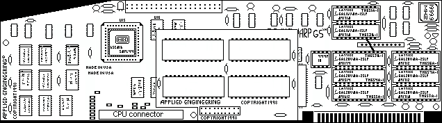
Here is a drawing I did of a Transwarp GS. If you put a real TWGS up to my computer monitor, it is a perfect fit. I spent a few hours on the drawing.
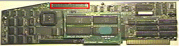
Have you ever wondered what the 40 pin connector on the top of the TWGS accelerator board is for?

Here is a quick look at the famous 40 pin connector on the TranswarpGS accelerator card. This is what was easy to
trace in a few minutes by sight. It is a view from the back of the card. The connector is directly connected to the 65816 CPU. Now I need a pinout for the PLCC socket. (got it. see below)
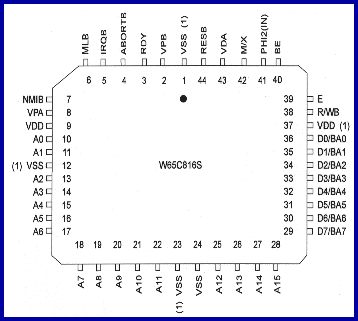
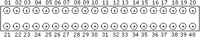
Here's the pinout from WDC (http://westerndesigncenter.com/ch816S.html):
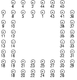
I got the PLCC socket pinout from:
http://www.methode.com/connector/pdfsforconnector/plcc.pdf
The one on the right is backwards (horizontally flipped) to match the above schematic.
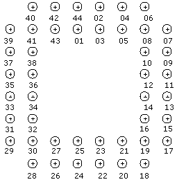
Here is the pinout of the PassTru connector,looking at the front (cache/cpu side). I don't know the conventions for numbering connectors, but I numbered it as I've seen on other connectors.
Here's a chart of the connections. Almost all of the CPU leads have a direct connection to the TWGS CPU passthrough connector. It took about an hour and a half to trace the leads. If you use this information for anything, or find it interesting, send me an email! (I just fixed the error that was introduced when I incorrectly reversed the PLCC socket pinout.)
TWGS CPU PASSTHRU PINOUT
| TWGS connector |
CPU pin |
function |
| 01 |
22 |
A11 |
| 02 |
21 |
A10 |
| 03 |
20 |
A9 |
| 04 |
19 |
A8 |
| 05 |
18 |
A7 |
| 06 |
17 |
A6 |
| 07 |
16 |
A5 |
| 08 |
15 |
A4 |
| 09 |
14 |
A3 |
| 10 |
13 |
A2 |
| 11 |
11 |
A1 |
| 12 |
10 |
A0 |
| 13 |
?? |
?? |
| 14 |
08 |
VPA |
| 15 |
07 |
NMIB |
| 16 |
06 |
MLB |
| 17 |
05 |
IRQB |
| 18 |
?? |
?? |
| 19 |
?? |
?? |
| 20 |
02 |
VPB |
| 21 |
01 |
VSS |
| 22 |
25 |
A12 |
| 23 |
26 |
A13 |
| 24 |
27 |
A14 |
| 25 |
28 |
A15 |
| 26 |
29 |
D7/BA7 |
| 27 |
30 |
D6/BA6 |
| 28 |
31 |
D5/BA5 |
| 29 |
31 |
D4/BA4 |
| 30 |
33 |
D3/BA3 |
| 31 |
34 |
D2/BA2 |
| 32 |
25 |
D1/BA1 |
| 33 |
36 |
D0/BA0 |
| 34 |
38 |
R/WB |
| 35 |
39 |
E |
| 36 |
40 |
BE |
| 37 |
42 |
PHI2 (IN) |
| 38 |
42 |
M/X |
| 39 |
43 |
VDA |
| 40 |
44 |
RESB |
Have any ideas for the use of the CPU passthru? Let me know!
Email Osites
Or click here to read a few ideas I had as I was designing the page.
COMING SOON: (they're here! ) Cache connector pinouts (all I have to do is upload them. They are already drawn up.). I have cache, passthru schematics. Next thing I want to do is draw up the schematic for the GAL chips and how/where then connect elsewhere on the TWGS.
More TWGS stuff here
Help me upgrade my RAMFACTOR here
The beginning of an online PC Transporter manual here